


针对Altium Designer 13的新用户,不清楚怎样制作线路板封装的问题,下面小编介绍下Altium Designer 13制作线路板封装的详细操作流程。
Altium Designer 13制作线路板封装的详细操作流程

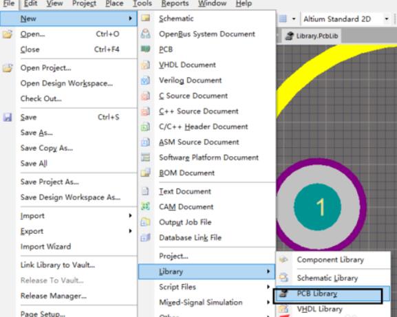
打开Altium designer,file新建一个PCB库
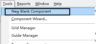
点击Tools创建新的器件
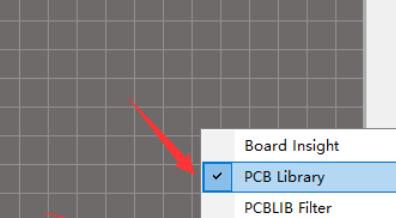
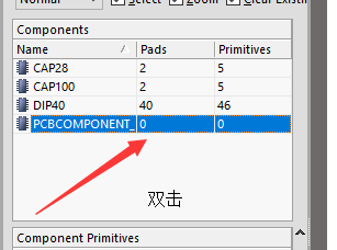
点击右下角的SCH选中PCB Library弹出器件
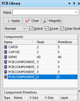
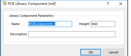
双击器件修改名称
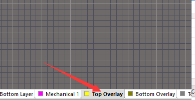
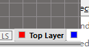
切换到top overlay丝印层进行绘制
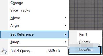
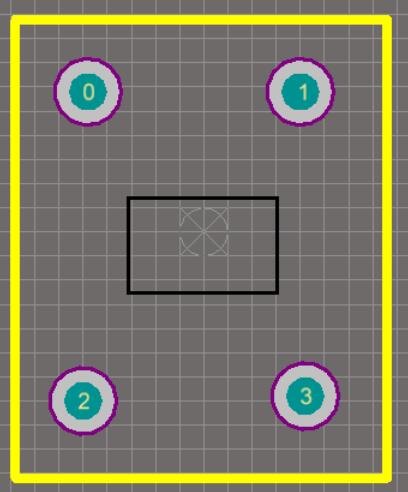
在Edit中的Location绘制坐标原点
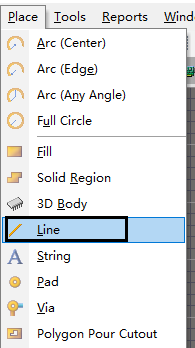
选择place中的Line进行绘制
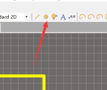
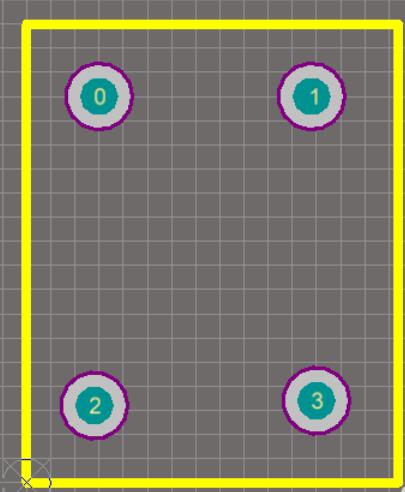
之后绘制焊盘,切换到顶层Top Layer
按Tab进行属性更改
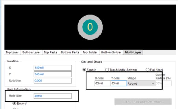
焊盘根据文档进行绘制
最后将坐标原点放置到器件中心
上文就是Altium Designer 13制作线路板封装的详细操作流程,赶快试试看吧。