


如何用protel99se给PCB铺地呢?很多小伙伴都在问这个问题,今日在这里就为你们带来了protel99se给PCB铺地的具体操作方法。
protel99se给PCB铺地的操作教程

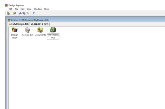
打开protel99se。
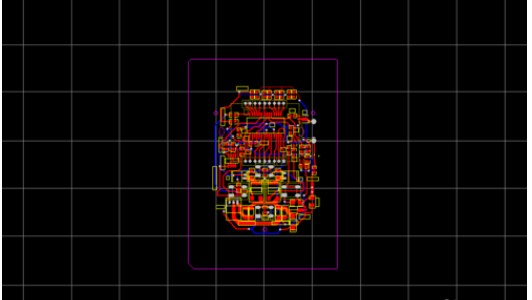
画好PCB,需要连接VSS的地方可以暂时不用连接。
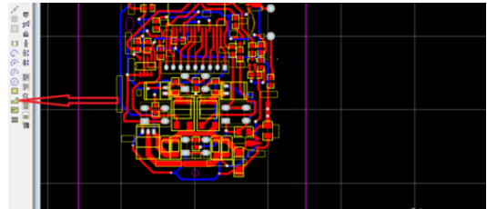
点击"PlacePolygonPlane"弹出铺地选择设置。
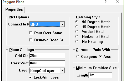
设置 connet to net 选择GND。
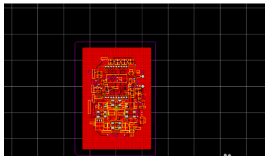
选择电路板顶层,画线把需要铺地的区域包围起来即可铺地。
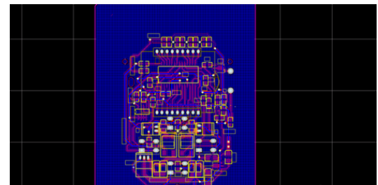
使用同样的方法,切换到电路板底层,铺地即可。
根据上文为你们讲解protel99se给PCB铺地的具体操作方法,你们是不是都学会啦!